How light carves the microscopic architecture of every modern computer chip
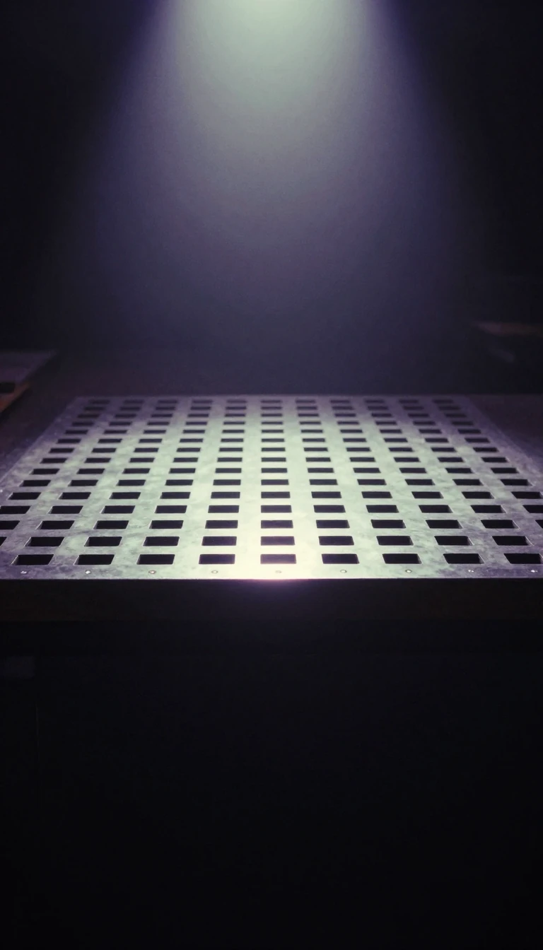
In short: Photolithography is the precise engine behind the semiconductor industry. By using light to project intricate patterns onto silicon, engineers can etch complex circuits at the nanoscale. This process, which repeats dozens of times for a single chip, transforms simple wafers into the powerful microprocessors that drive our digital world.
At its core, photolithography is a sophisticated method for transferring patterns onto a substrate, typically a silicon wafer. The process begins by coating the wafer with a light-sensitive material known as photoresist. A mask, featuring the desired circuit design in chrome on glass, acts as a stencil. When ultraviolet light is directed through this mask, it selectively exposes the photoresist. Depending on the chemical formulation, the light either makes the resist soluble or insoluble in a developer solution, effectively creating a physical map of the circuit on the wafer surface.
Once the pattern is developed, the exposed or unexposed areas are removed, leaving the underlying wafer vulnerable. This allows for subsequent modifications, such as etching or depositing new materials into the exposed gaps. After these structural changes are complete, the remaining photoresist is stripped away. In the production of advanced integrated circuits, this entire cycle may be repeated up to 50 times using different masks, building up the complex, multi-layered architecture required for modern computing.
The precision of this technique is largely dictated by the wavelength of the light source. As manufacturing demands smaller features, the industry has shifted toward shorter wavelengths, moving from standard ultraviolet to extreme ultraviolet and X-ray sources. While the field is highly mature, it remains constrained by the need for perfectly flat surfaces and pristine, clean-room environments. Despite these challenges, photolithography remains the most efficient way to mass-produce chips, enabling the creation of intricate, microscopic patterns across an entire wafer in a single, rapid operation.
Opens the Intellect+ feed with this card first. Swipe up for the next one.
Sources
- Summary by Intellect · source: Photolithography | Britannica
- Also: Photolithography
To cite this card, link to https://intellectplus.co.uk/app/technology-photolithography.
How we source, check and correct cards: Editorial standards.
General information, not professional advice. Spotted an error? Flag the card or see corrections and complaints.
Intellect Plus is a visual educational discovery platform for exploring fascinating facts and ideas. Brain Food, Not Brain Rot. What is Intellect Plus?
Related
More in Optical technology · More in Technology · Latest · A–Z · All topics
