Photonic crystals: The nanostructures that manipulate light like semiconductors manipulate electrons
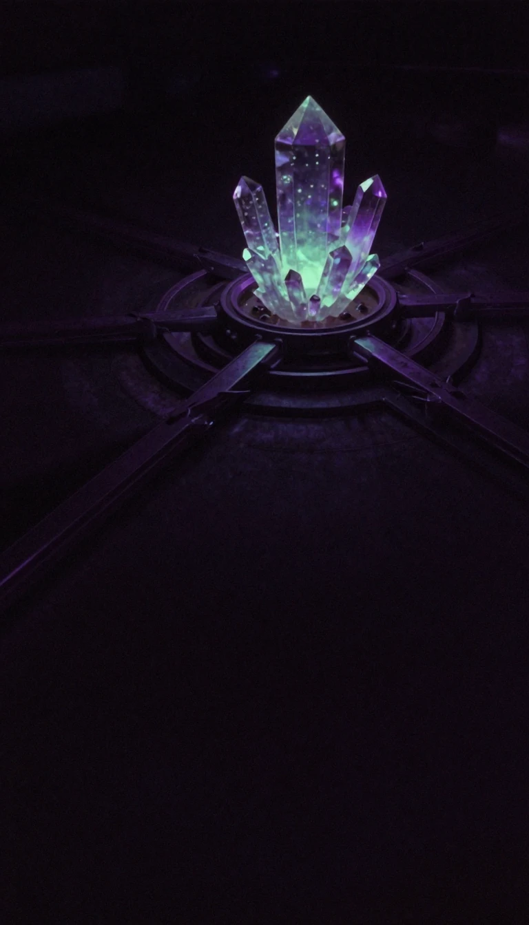
In short: Imagine a material that forces light to bend around sharp corners or traps it entirely. Photonic crystals achieve this by using periodic nanostructures to create band gaps, effectively controlling light propagation. From structural coloration in nature to the future of optical computing, these materials are redefining how we engineer light.
A photonic crystal is an optical nanostructure characterized by a periodic change in its refractive index. This structure influences light propagation in a manner analogous to how atomic lattices in semiconductors dictate electron conductivity. By creating regularly repeating regions of high and low refractive index, these crystals can inhibit spontaneous emission or create omni-directional mirrors. When light encounters these interfaces, destructive interference occurs, resulting in photonic band gaps—ranges of wavelengths that are disallowed from propagating through the material.
The history of these structures dates back to 1887, when Lord Rayleigh studied periodic multi-layer dielectric stacks, now recognized as one-dimensional photonic crystals. However, the field gained significant momentum in 1987 following milestone papers by Eli Yablonovitch and Sajeev John, which explored high-dimensional periodic optical structures. Today, fabrication methods vary by dimension: one-dimensional crystals are often made via thin-film deposition, while two-dimensional structures, such as photonic-crystal fibers, are produced using photolithography or etching. Three-dimensional fabrication remains more complex, often involving techniques like direct laser writing, self-assembly of spheres, or the construction of 'woodpile' structures.
The potential applications for photonic crystals are vast. In telecommunications, photonic-crystal fibers are already commercially available. Researchers are also investigating photonic crystal slabs—semiconductor materials patterned to combine photonic and electronic processing on a single chip. Furthermore, by introducing defects into the crystal lattice, scientists can create nanosize cavities that act as resonators, capable of delaying light pulses or enhancing emission from embedded materials. While challenges in mass production and precision remain, the field continues to expand through biomimetics, drawing inspiration from natural structures like the scales of beetles and the wings of butterflies.
Crucially, the analysis of these crystals relies on classical physics, despite the term 'photonic' referencing the quantization of light. Because electromagnetic fields exhibit scale invariance, early research often utilized the microwave regime, where structures could be built on the centimeter scale rather than the nanometer scale required for visible light. As fabrication techniques mature, these materials promise to revolutionize optical computing and photovoltaic efficiency.
Opens the Intellect+ feed with this card first. Swipe up for the next one.
Sources
- Summary by Intellect · source: Photonic crystal
- Also: www.nature.com — Photonic crystals - Latest research and news | Nature
To cite this card, link to https://intellectplus.co.uk/app/science-photonic-crystal.
How we source, check and correct cards: Editorial standards.
General information, not professional advice. Spotted an error? Flag the card or see corrections and complaints.
Intellect Plus is a visual educational discovery platform for exploring fascinating facts and ideas. Brain Food, Not Brain Rot. What is Intellect Plus?
Related
More in Waves · More in Science · Latest · A–Z · All topics
