How adding microscopic impurities transforms pure silicon into the engine of modern technology
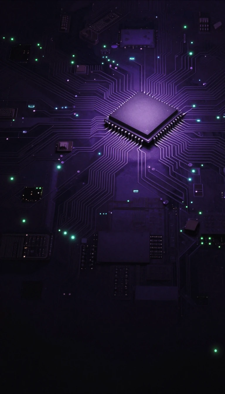
In short: Pure silicon is a poor conductor, but by intentionally introducing tiny amounts of specific impurities—a process called doping—engineers can precisely modulate its electrical properties. This delicate manipulation of atomic structure creates the p-n junctions that power everything from your smartphone to the complex integrated circuits of modern computing.
Doping is the deliberate introduction of impurities into an intrinsic semiconductor to alter its electrical, optical, and structural behavior. At its core, this process relies on the periodic table. By adding Group V elements like phosphorus to silicon, engineers introduce extra valence electrons that act as donors, creating n-type semiconductors. Conversely, adding Group III elements like boron creates 'holes'—missing electrons that act as acceptors—resulting in p-type material. These dopants create allowed energy states within the material's band gap, very close to the conduction or valence bands, allowing room temperature to thermally ionize the atoms and generate free charge carriers.
The concentration of these dopants is remarkably precise. While intrinsic silicon contains roughly 5x10^22 atoms per cubic centimeter, doping levels typically range from 10^13 to 10^18 atoms per cubic centimeter. When doping reaches levels above 10^18, the material becomes a degenerate semiconductor, behaving more like a metal than a traditional semiconductor. This high-level doping is essential for integrated circuits, where n+ or p+ regions are used to replace metal components. The ability to control these concentrations allows for the creation of band bending at interfaces, a fundamental mechanism behind the operation of diodes and transistors.
Techniques for doping have evolved significantly since the early empirical observations of the 1880s and 1930s. Modern manufacturing uses methods like thermal diffusion, where wafers are heated in furnaces with chemical sources like Boron tribromide, or ion implantation, which offers superior controllability for large-scale production. Other specialized methods include vapor-phase epitaxy and even neutron transmutation doping, which uses nuclear reactors to convert silicon isotopes into phosphorus for extreme uniformity. Whether through standard CMOS technology or specialized applications like gallium-doped solar cells, doping remains the primary tool for tailoring the physical reality of silicon to meet the demands of modern electronics.
Opens the Intellect+ feed with this card first. Swipe up for the next one.
Sources
- Summary by Intellect · source: Doping (semiconductor)
To cite this card, link to https://intellectplus.co.uk/app/technology-doping-semiconductor.
How we source, check and correct cards: Editorial standards.
General information, not professional advice. Spotted an error? Flag the card or see corrections and complaints.
Intellect Plus is a visual educational discovery platform for exploring fascinating facts and ideas. Brain Food, Not Brain Rot. What is Intellect Plus?
Related
More in Optical technology · More in Technology · Latest · A–Z · All topics
