Micro-electromechanical systems are the invisible machines powering our modern digital world
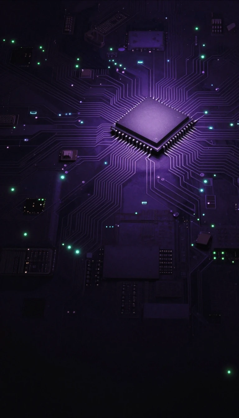
In short: MEMS are microscopic devices that bridge the gap between electronic data processing and physical interaction. Ranging from 20 micrometres to a millimetre, these tiny machines use silicon, polymers, or metals to sense, move, and measure. They are the hidden engines behind everything from pressure sensors to advanced optical displays.
The concept of machines at the micro-scale predates the technology required to build them, famously highlighted in Richard Feynman's 1959 lecture. Practical fabrication only arrived when engineers adapted semiconductor manufacturing techniques—such as photolithography, etching, and thin-film deposition—to create mechanical structures alongside integrated circuits. The term MEMS was officially coined in 1986 by S.C. Jacobsen and J.E. Wood in a proposal to DARPA, marking the formal birth of a field that now spans from simple sensors to complex arrays.
Silicon remains the industry standard for MEMS, prized for its near-perfect Hookean properties. In its single-crystal form, silicon exhibits virtually no hysteresis or energy dissipation, allowing for billions of cycles of repeatable motion without fatigue. While silicon is expensive to produce, its ability to integrate electronic functionality makes it ideal for high-performance applications like accelerometers. For lower-cost or specialized needs, manufacturers turn to polymers for microfluidic devices or metals like gold and nickel for high-reliability electrical components.
The precision of MEMS relies on sophisticated etching techniques. Wet etching, which uses chemical solutions to dissolve material, allows for complex 3D structures based on crystallographic orientation. Conversely, dry etching—specifically Deep Reactive Ion Etching (DRIE)—uses plasma to achieve vertical sidewalls and extreme aspect ratios. The 'Bosch process,' a key DRIE method, alternates gas compositions to protect sidewalls with polymers while etching floors, enabling engineers to carve deep, narrow features into silicon wafers with unprecedented accuracy.
Today, MEMS technology continues to evolve, merging into the nanoscale with NEMS. From biosensors that measure fluid viscosity to disposable blood testing cartridges, these devices are essential to modern industry. By mastering the manipulation of materials at the micron scale, researchers have created a versatile toolkit that allows us to interact with the physical environment through the lens of digital precision.
Opens the Intellect+ feed with this card first. Swipe up for the next one.
Sources
- Summary by Intellect · source: MEMS
To cite this card, link to https://intellectplus.co.uk/app/technology-mems.
How we source, check and correct cards: Editorial standards.
General information, not professional advice. Spotted an error? Flag the card or see corrections and complaints.
Intellect Plus is a visual educational discovery platform for exploring fascinating facts and ideas. Brain Food, Not Brain Rot. What is Intellect Plus?
Related
More in Machinery and tools · More in Technology · Latest · A–Z · All topics
