How packing billions of transistors onto silicon chips changed the world forever
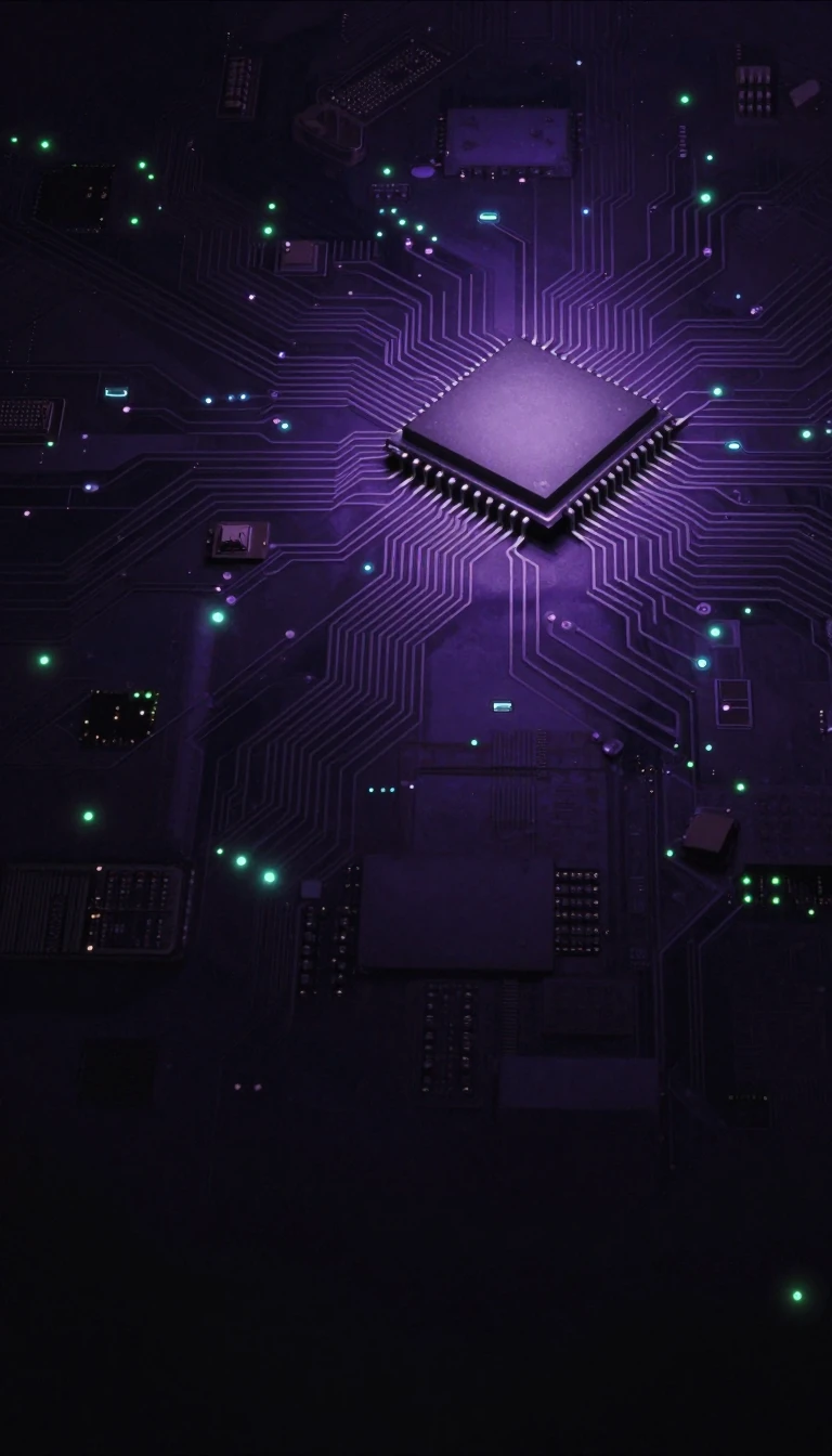
In short: Very-large-scale integration, or VLSI, is the engine of modern computing. By shrinking millions and eventually billions of transistors onto a single semiconductor chip, engineers moved electronics from bulky, slow circuits to the high-speed microprocessors that power everything from personal computers to the latest breakthroughs in quantum photonic research.
The evolution of integrated circuits began in the 1960s, progressing from small-scale integration (SSI) to medium-scale (MSI) and large-scale integration (LSI). By the 1970s, the industry reached the VLSI era, defined by the ability to pack tens of thousands of transistors onto one chip. This density grew exponentially, following the trend famously described by Moore's law. By the 1990s, chips held over 3 million transistors, and by the 2010s, that number reached billions, all while maintaining the same physical footprint.
The dominance of VLSI is largely due to the metal-oxide-semiconductor field-effect transistor (MOSFET). These devices are easily scaled down, consume minimal power, and offer high manufacturing yields. Designing these chips is a complex, multi-stage process involving functional specifications, hardware description languages, and sophisticated computer-aided design tools. Designers must navigate challenges like process variation, where photolithography limits make it difficult to achieve perfect doping and wire etching, requiring extensive simulation before production.
Beyond classical computing, VLSI is now pushing into the quantum realm. Researchers are using VLSI techniques to fabricate graph-theoretical quantum photonic devices on silicon substrates. One such device, measuring just 12 mm by 15 mm, integrates 2,446 components—including photon-pair sources, phase shifters, and delay lines—to perform complex quantum experiments. By mapping abstract graph theory onto physical optical pathways, these chips can generate multipartite entanglement and solve computational problems that are otherwise mathematically intractable.
This shift from simple logic gates to massive, programmable architectures highlights the versatility of silicon fabrication. Whether it is a standard microprocessor or a specialized quantum photonic processor, the ability to integrate vast numbers of components onto a single wafer remains the fundamental constraint and enabler of technological progress.
Opens the Intellect+ feed with this card first. Swipe up for the next one.
Sources
- Summary by Intellect · source: Very-large-scale integrated quantum graph photonics - Nature Photonics
- Also: Very large-scale integration | electronics | Britannica
- Also: Very-large-scale integration
To cite this card, link to https://intellectplus.co.uk/app/technology-very-large-scale-integration.
How we source, check and correct cards: Editorial standards.
General information, not professional advice. Spotted an error? Flag the card or see corrections and complaints.
Intellect Plus is a visual educational discovery platform for exploring fascinating facts and ideas. Brain Food, Not Brain Rot. What is Intellect Plus?
Related
More in Electronics · More in Technology · Latest · A–Z · All topics
