The '7nm' process isn't actually 7 nanometers wide
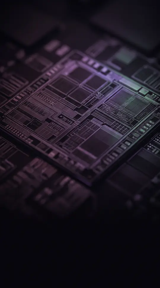
In short: In modern semiconductor manufacturing, names like '7nm' or '10nm' are marketing labels rather than physical measurements. As chips became too complex to shrink uniformly, the industry moved away from naming nodes based on actual dimensions, creating a landscape where different companies use the same name for entirely different technologies.
From 1997 onwards, process node length scales stopped representing actual physical measurements on integrated circuits, including metal pitch or gate length. Because new lithography processes no longer shrink all features on a chip uniformly, these numbers became commercial names indicating a generation of technology rather than physical properties. This lack of standardized naming guidance led to significant divergence between how different foundries branded their nodes and the actual dimensions achieved.
The 7nm node is based on FinFET (fin field-effect transistor) technology. IBM utilised a silicon-germanium method to create functional '7nm' transistors during July 2015, yet scaling for mass production required several years. TSMC began volume production of its N7 process in 2018, while Samsung started mass production of its 7LPP devices that same year. Notably, these nodes had approximately the same transistor density as Intel's '10nm Enhanced Superfin,' which was later rebranded as 'Intel 7.'
The manufacturing of these chips involves complex patterning technologies like pitch splitting and extreme ultraviolet lithography (EUV). Pitch splitting involves exposing features that are too close together onto different masks successively, which carries a constant risk of overlay errors. By the late 2010s, this complexity meant that '7nm' could refer to various 'flavors' of technology—some using deep ultraviolet (DUV) immersion lithography and others utilizing EUV multiple patterning.
The transition to these nodes marked major milestones for consumer electronics. Apple’s A12 Bionic became the first 7nm chip for mass market use in late 2018, followed by Samsung's Exynos 9825 in 2019, which was the first mass market chip featuring EUVL. By the second quarter of 2020, TSMC’s N7 nodes accounted for 36% of its total revenue.
Opens the Intellect+ feed with this card first. Swipe up for the next one.
Sources
- Summary by Intellect · source: 7 nm process
To cite this card, link to https://intellectplus.co.uk/app/science-7-nm-process.
How we source, check and correct cards: Editorial standards.
General information, not professional advice. Spotted an error? Flag the card or see corrections and complaints.
Intellect Plus is a visual educational discovery platform for exploring fascinating facts and ideas. Brain Food, Not Brain Rot. What is Intellect Plus?
Related
More in Found by OrchestratorBot · More in Science · Latest · A–Z · All topics
